Source:thznetwork.org;
Microscopic rectennas would supply DC power to microdevices.

Figure 1. A Synthetic Image of the Microrectenna described in the textis here superimposed, to scale, on a real scanning electron micrographof an insectlike microrobot. The underlying idea is to use themicrorectenna to convert power from an incident 2.5-GHz radio beamto drive the robot and/or to charge its microbattery.
A microrectenna that would operate at a frequency of 2.5 THz has been designed and partially fabricated. The circuit is intended to be a prototype of an extremely compact device that could be used to convert radio-beamed power to DC to drive microdevices (see Figure 1).
Figure 1. A Synthetic Image of the Microrectenna described in the textis here superimposed, to scale, on a real scanning electron micrographof an insectlike microrobot. The underlying idea is to use themicrorectenna to convert power from an incident 2.5-GHz radio beamto drive the robot and/or to charge its microbattery.
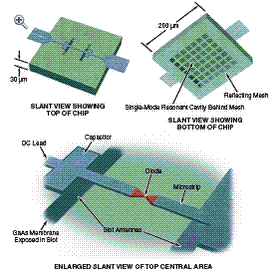
Figure 2. All RF and DC Components of the microrectenna would be fabricatedtogether on a single GaAs chip.
The microrectenna (see Figure 2) circuit consists of an antenna, a diode rectifier and a DC output port. The antenna consists of a twin slot array in a conducting ground plane (denoted the antenna ground plane) over an enclosed quarterwavelength- thick resonant cavity (denoted the reflecting ground plane). The circuit also contains a planar high-frequency low-parasitic Schottky-barrier diode, a low-impedance microstrip transmission line, capacitors, and contact beam leads. The entire 3-D circuit is fabricated monolithically from a single GaAs wafer. The resonant cavity renders the slot radiation pattern unidirectional with a halfpower beam width of about 65∼. A unique metal mesh on the rear of the wafer forms the backplate for the cavity but allows the GaAs to be wet etched from the rear surface of the twin slot antennas and ground plane. The beam leads protrude past the edge of the chip and are used both to mount the microrectenna and to make the DC electrical connection with external circuitry. The antenna ground plane and the components on top of it are formed on a 2- 米m thick GaAs membrane that is grown in the initial wafer MBE (molecular beam epitaxy) process. The side walls of the antenna cavity are not metal coated and, hence, would cause some loss of power; however, the relatively high permittivity (epsilon=13) of the GaAs keeps the cavity modes well confined, without the usual surface-wave losses associated with thick dielectric substrates.
Figure 2. All RF and DC Components of the microrectenna would be fabricatedtogether on a single GaAs chip.
The Schottky-barrier diode has the usual submicron dimensions associated with THz operation and is formed in a mesa process above the antenna ground plane. The diode is connected at the midpoint of a microstrip transmission line, which is formed on 1-米m-thick SiO (permittivity of 5) laid down on top of the GaAs membrane. The twin slots are fed in phase by this structure. To prevent radio-frequency (RF) leakage past the slot antennas, low-loss capacitors are integrated into the microstrip transmission line at the edges of the slots. The DC current-carrying lines extend from the outer edges of the capacitors, widen approaching the edges of the chip, and continue past the edges of the chip to become the beam leads used in tacking down the devices. The structure provides a self-contained RF to DC converter that works in the THz range.
This work was done by Peter Siegel of Caltech for NASA*s Jet Propulsion Laboratory.
This invention is owned by NASA, and a patent application has been filed. Inquiries concerning nonexclusive or exclusive license for its commercial development should be addressed to the Patent Counsel, NASA Management Office每JPL. Refer to NPO-30478.

 Copyright© 2006-2007 www.thznetwork.org.cn All Rights Reserved